#Introduction: Why OLED Innovation Needs Faster Chemistry
Organic light emitting diodes (OLEDs) are now ubiquitous in our daily life, with devices ranging from smartphones to laptops, monitors and TVs all using this key technology to emit light directly, instead of only selectively transmitting light through individual pixels like liquid crystal displays (LCDs).
During OLED operation, electrons injected from the cathode and holes injected from the anode migrate through organic transport layers before recombining in the emissive layer to form excitons that release energy as light. The molecular structure, purity, and functional groups of these materials dictate charge mobility, exciton stability, and emission color, making precise molecular design and synthesis central to OLED performance.
The structure of an OLED device is quite complex, but we can isolate the most important materials contributing to the light output to a few critical layers:
Anode/Cathode: Typically made up of inorganics like indium tin oxide (ITO) or low-work function metals like magnesium, depending on the respective need for transparency. These layers serve as the electrodes where holes and electrons are injected into the device.
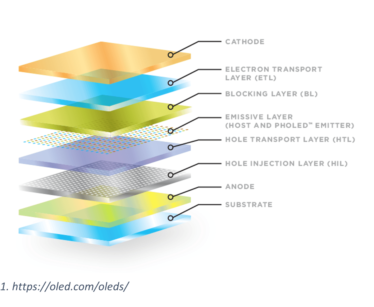 Simplified example of OLED internal layer structure. Courtesy of OLED.com/OLEDs
Hole Injection Layer (HIL): This layer facilitates hole injection from the anode into the other organic layers. Common materials include poly(3,4-ethylenedioxythiophene):poly(styrenesulfonate) (PEDOT:PSS) for solution-processed devices, or small molecules like copper phthalocyanine (CuPc), or inorganics such as molybdenum oxide (MoO₃) for vacuum-deposited devices (more on this differentiation later).
Hole Transport Layer (HTL): This layer transports holes toward the emission zone while blocking electrons. Typical materials include benzinidine-based compounds like TPD and NPB, or spiro-linked aromatics such as spiroOMeTAD.
Emission Layer (EML): This is where light generation occurs through radiative recombination of electrons and holes. The layer often consists of a host material doped with emissive guest molecules. Host materials include carbazole derivatives like 4,4'-N,N'-dicarbazolebiphenyl (CBP) or anthracene derivatives. Emissive dopants vary by color: fluorescent dyes like Alq₃ (green) and phosphorescent complexes like Ir(ppy)₃ (green) or FIrpic (blue).
Electron Transport Layer (ETL): This layer transports electrons from the cathode toward the emission zone while blocking holes. Common materials include quinolines such as Alq₃, benzimidazoles such as TPBi, and many other cycloaromatic nitrogenated compounds like BPhen, BCP, and TmPyPB.
Electron Injection Layer (EIL): This thin layer improves electron injection from the cathode. It can consist of both inorganics such as lithium fluoride (LiF) and cesium fluoride (CsF), or organic and organometallic materials like 8-quinolinolato lithium (Liq).
Modern OLED devices are also made with additional layers such as hole-blocking layers (HBL) or electron-blocking layers (EBL) to confine charge carriers within the emission zone, improving efficiency. The specific molecular structures and layer thicknesses can be carefully optimized to balance charge injection, transport, and confinement to maximize device performance.
Intentional design of the molecular structure for each of the layers mentioned above is fundamental to the performance of the overall device. Recent experimental results such as those presented by Nagamura et al. show how sensitive OLED performance characteristics, such as mobilities and lifetimes, can be to simple molecular modifications. For example, the paper demonstrates the results of changes in position and quantity of moiety types using dibenzofuran additions – hole mobility decreased 60% and operation lifetime increased 17% with two additional dibenzofuran groups.
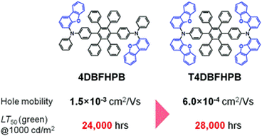 Comparison of hole mobility and operation lifetime at 50% of initial luminance (LT50) before and after dibenzofuran additions.
Given the critical roles played by these intricate organic molecules, macromolecules, and organometallic complexes, custom molecule synthesis remains a cornerstone of OLED innovation. The next frontier lies in solving two enduring challenges: creating stable, high-efficiency phosphorescent blue emitters and developing solution-processable device architectures that simplify large-scale manufacturing. Meeting these challenges will determine how far OLED technology can continue to evolve.
#The Blue Challenge: Phosphorescent Stability for Device Efficiency
Long considered a 'holy grail' development, commercialized blue phosphorescent materials are a highly sought after innovation to dramatically reduce power consumption of the blue subpixel. With sufficiently long lifetimes, these materials could replace the fluorescent emitters commonly found in current consumer electronic displays. Many challenges exist in creating a novel material that is both sufficiently pure and stable in color, as well as long lasting at high at the high luminance (>1000 Cd/m2) typically seen in modern consumer electronics. However, the key issue in focus currently is the development of materials with increased bond dissociation energies that still yield sufficiently pure blue emission spectra.
In 2022, Sun et al. showed how simple moiety modifications can dramatically improve the lifetime of phosphorescent blue OLED devices while maintaining color purity by using novel dopant and transport materials. The unique triphenylsilyl-modified compounds in the paper demonstrated great progress in stabilizing bond dissociation energies in the carbazole HTL and ETL materials, but the major advance came from the ditertbutyl phenyl addition to the novel dopant material. By combining both the triphenylsilyl-based transport layers and the ditertbutyl phenyl modified host, the authors were able to demonstrate an LT70 of over 1100 hours at 1000 cd/m2, more than 50x longer compared to other leading phosphorescent blue host materials.
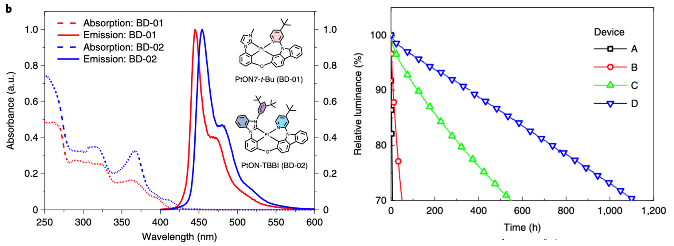 Improved blue OLED performance through use of novel dopant and transport materials.
In the next generation of emergent phosphorescent blue OLED materials, the ability to rapidly screen new compounds mixed with more stereotypical materials, such as carbazole-based solutions, is key. This is exemplified by the success of the ditertbutyl and triphenylsilyl moieties mentioned above. LG Display presented research at Display Week 2025 that underscored progress being made in commercializing these phosphorescent blues for lower power in tandem OLED architectures. This is where fluorescent blue stability still needs further development.
#Solution-Processable Materials for Inkjet Printed OLEDs
As OLED manufacturing scales toward larger displays and higher-resolution panels, the methods used to deposit and pattern thin organic layers have become a critical bottleneck. Traditional techniques rely on precisely controlled vacuum-based processes that, while effective, can be costly and difficult to scale. To understand where new opportunities lie, it's helpful to look at how current deposition approaches – particularly vacuum thermal evaporation (VTE) and fine metal mask (FMM) patterning – compare with emerging solution-based techniques such as inkjet printing. The current industry standard for fine patterning of OLED pixel arrays uses VTE through precision FMMs. However, this process is expensive and limits how large OLED substrates can become, especially as manufacturers move toward larger area displays. Additionally, challenges such as decreasing aperture areas in high-resolution devices and material waste during conformal VTE mean that new deposition methods must be explored for continued OLED adoption, particularly in large-display applications.
Inkjet printing OLED layers represents a promising solution to these challenges, while also eliminating the equipment cost and scaling issues associated with VTE at large substrate sizes. However, many traditional materials require process optimization to achieve sufficient solubility in the solvents used for printing. Wei et al sought to solve this problem by modifying the pyridine-linkage orientation in their material design, dramatically improving solubility in dichloroethane while maintaining similar optoelectronic properties in a model top-emission device. Their study showed that a 2,6-pyridine core not only increases solubility by up to 8x but it also provides a much higher surface energy (~40 mN/m), improving subsequent ink-jet printing steps in non-aqueous media. This main chain positioning is just one way of modulating solubility, but side-chain moiety modification is another avenue that can be explored in the case of known target solvent systems to further improve solvent compatibility.
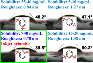 Solubility changes resulting from pyridine-linkage orientation modifications.
#Summary and Future Outlook
At the heart of every OLED innovation lies a precise interplay of electrons and holes – an interaction shaped entirely by the chemistry behind each layer. Both new molecule synthesis and small modifications to existing structures are essential pathways to discovering the next generation of OLED materials. In most cases, these compounds don't yet exist and require novel synthetic routes and careful evaluation of their scalability. As synthesis capabilities evolve, so does our ability to design molecules that channel charge, control recombination, and unlock new frontiers in display performance.
#About DigiChem
Advancing OLED performance isn't just a scientific challenge – it's a supply chain one. Many promising new materials stall between lab discovery and commercialization because sourcing custom intermediates or scaling synthesis is slow, opaque, and fragmented across vendors. DigiChem was built to close that gap, integrating molecular design, quoting, and synthesis execution into one seamless digital workflow—giving researchers an intelligent, data-driven way to design, order, and scale new OLED materials with unprecedented speed and transparency.
Explore how it works on our website.
Want more materials innovation insights? Subscribe to the DigiChem newsletter for updates on next-gen display chemistry.
#References
- Wei, Changting, et al. "Pyridine-based electron-transport materials with high solubility, excellent film-forming ability, and wettability for inkjet-printed OLEDs." ACS Applied Materials & Interfaces 9.44 (2017): 38716-38727. https://doi.org/10.1021/acsami.7b12190
- Sun, J., Ahn, H., Kang, S. et al. Exceptionally stable blue phosphorescent organic light-emitting diodes. Nat. Photon. 16, 212–218 (2022). https://doi.org/10.1038/s41566-022-00958-4
- Nagamura, Natsuo, et al. "A multifunctional hole-transporter for high-performance TADF OLEDs and clarification of factors governing the transport property by multiscale simulation." Journal of Materials Chemistry C 10.22 (2022): 8694-8701. https://doi.org/10.1039/D2TC00716A